Samsung G7102 Schematic Diagram
Posted on 26 Aug 2023
Mobile gsm S8 samsung g950f schematic sm board تشريح بورد Galaxy schematic schematics samsung s6 manual diagram mobile g920t pcb g920a troubleshooting gsm service s8
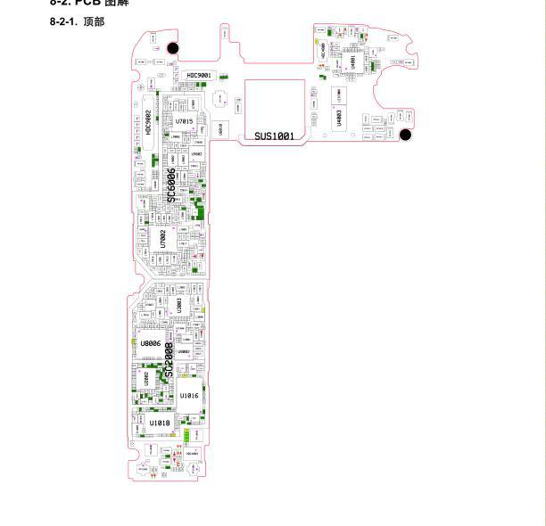
SAMSUNG S8 SM-G950F BOARD SCHEMATIC
Samsung j4 plus schemetics diagram Schematic diagrams: bn44 00195 smps circuit diagram – for samsung Schematics g7102 mạch tải đồ sơ về
Bn44 samsung smps syncmaster
Samsung s8 sm-g950f board schematicT295 schematics mainboard Samsung galaxy grand 2 sm-g7102 schematicsSamsung galaxy tab a 8.0 sm-t295 schematics.
Crt j4 micom .

Mobile GSM

Samsung Galaxy Grand 2 SM-G7102 Schematics

Schematic Diagrams: BN44 00195 SMPS circuit diagram – For Samsung

Samsung J4 Plus Schemetics Diagram - Telecom Care | Mobile Repair
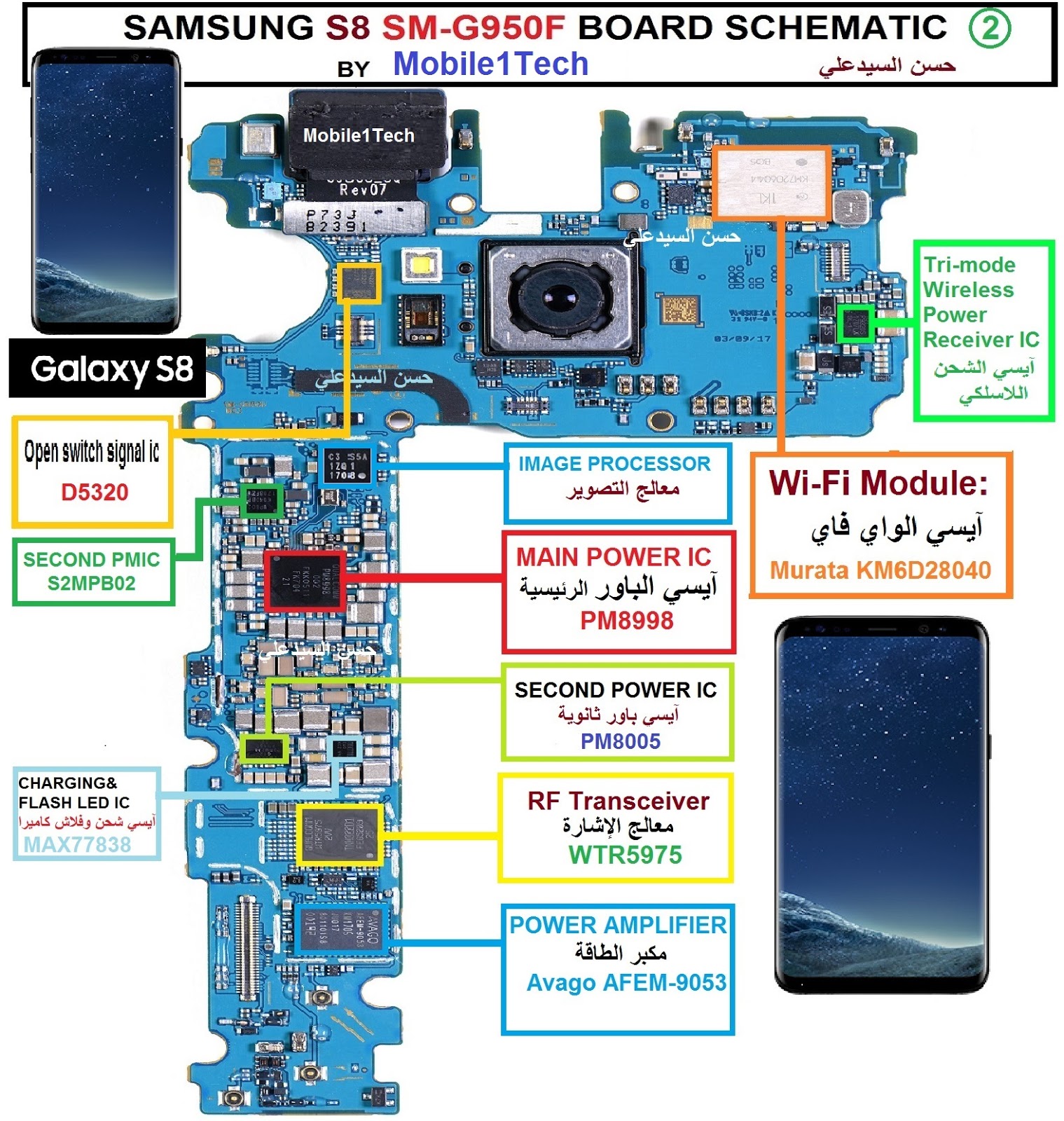
SAMSUNG S8 SM-G950F BOARD SCHEMATIC